PS Gnd ... what is that?

What is the funny terminal “PS Gnd” terminal next to the DC power input of the DÆ Phono Preamp v4.0 and what does it do?

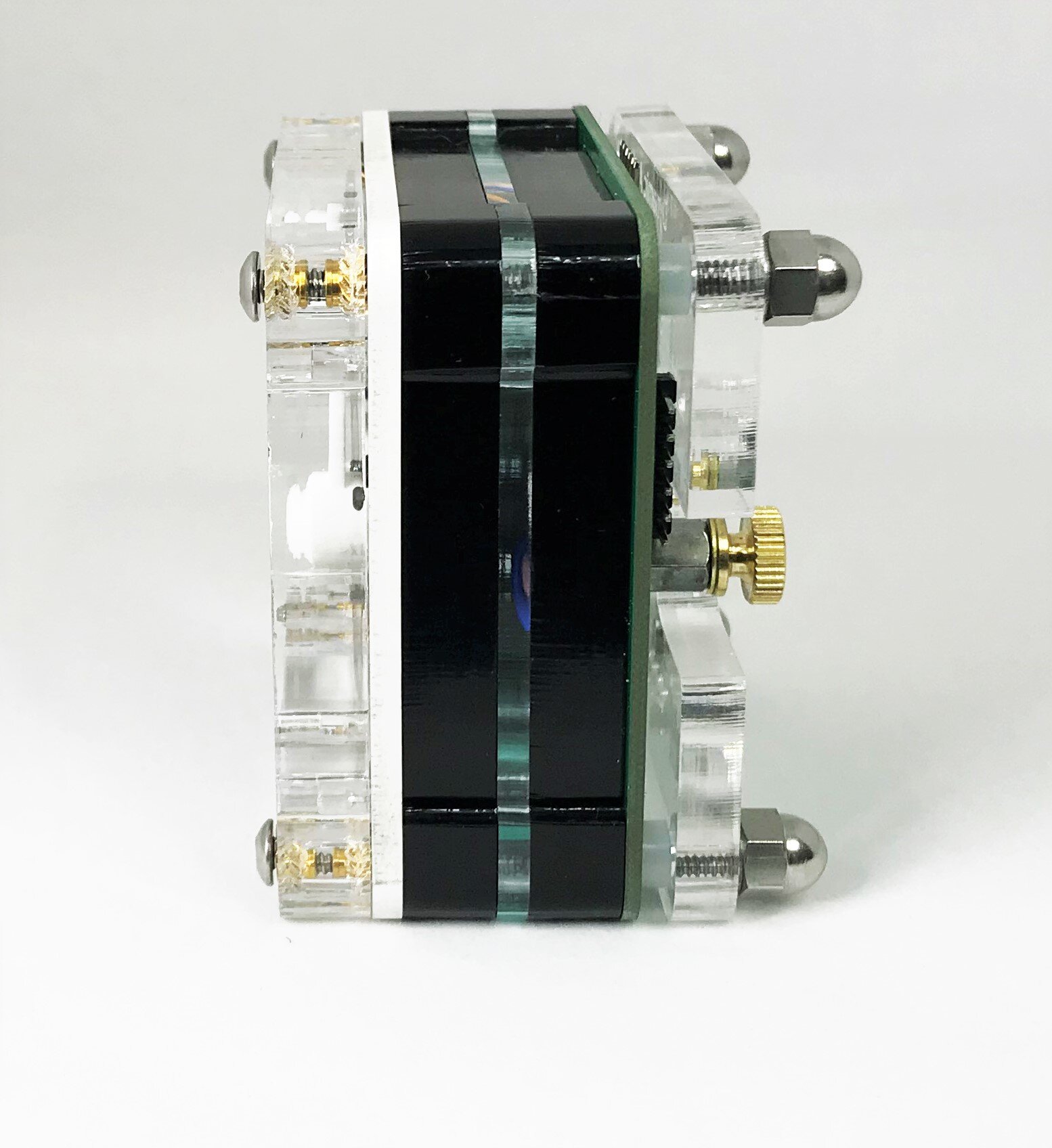
Photo of rear of DÆ Phono Preamp v4.0. Note terminal at the right labeled “PS Gnd”

PS Gnd stands for Power Supply Ground and it does quite a lot actually.

Measurements of the performance of the DÆ Phono Preamp v4.0 had to be very carefully done to get a clean measurement of the preamp alone. I paid particular attention to the cabling and grounding but no matter what I did, there was always a 60 Hz power line component above the background noise.

After much head scratching I discovered that the problem was caused by common mode noise from the switching power supply in the wall brick providing the 48 VDC to the preamp. “DC” or direct current is a relative term in this case as it direct current but it is certainly not noise free. Common mode noise was so pervasive that it even appeared at the output when the preamp was powered from it’s internal battery.

The solution was to add capacitor between the negative power supply terminal on the barrel connector and building ground to shunt the common mode noise away from the preamp. This YouTube video (click the words “YouTube video” to start the video) was very informative about common mode power supply noise and possible solutions. The video focuses on noise from a laboratory bench power supply. At about the the 21:40 mark the presenter describes a method to reduce the common mode noise that involves the simple addition of a capacitor at the output. In the DÆ Phono Preamp v4.0 circuit diagram (click the word “circuit” to see the schematic) of the rear connection board the PS Gnd connector and associated capacitor are parts J19 and C4 respectively.

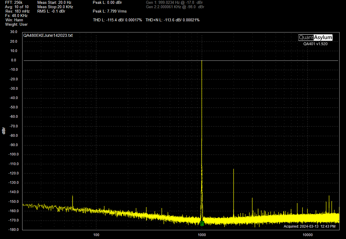
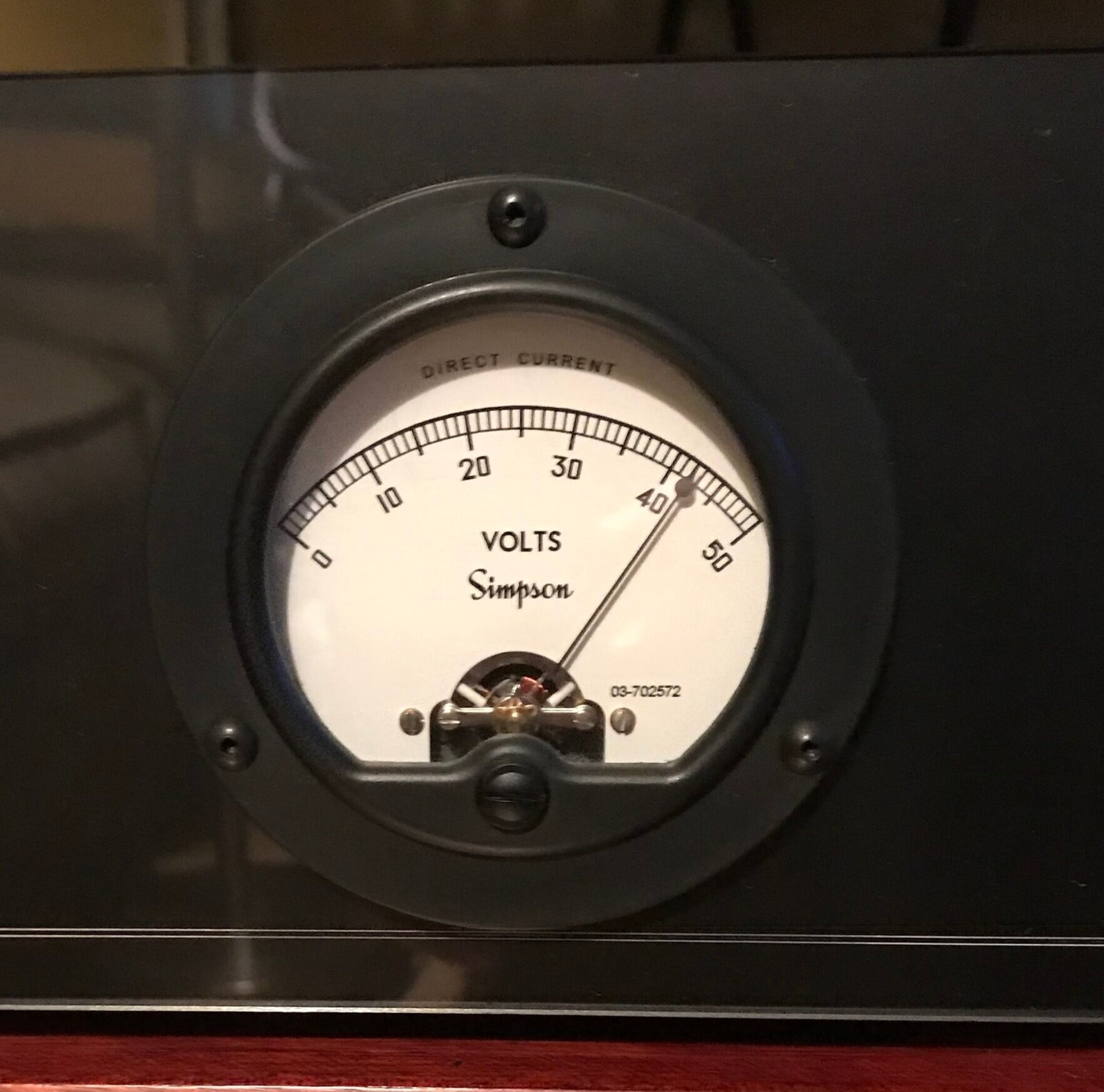
The following two graphs illustrate the effectiveness of connecting the PS Gnd terminal to the building ground. The first figure is the measured output of the DÆ Output Board v1.0 in an enclosure without a connection to the PS Gnd terminal.

DÆ Output Board v1.0 in the enclosure but without a connection to the PS Gnd terminal.

Pretty ugly isn’t it.

And with the PS Gnd terminal connected to building ground the results are…

DÆ Output Board v1.0 in the enclosure with a connection to the PS Gnd terminal.

Now that is more like it. The noise is reduced by many tens of decibels.

As a more common alternative to the PS Gnd terminal is a connection to the Chassis ground. The interference can be reduced by connecting the chassis directly to building ground using the Chassis Gnd terminal. Problem is this increases the possibility of forming a ground loop especially if the pre-amplifier or amplifier downstream of the DÆ Phono Preamp v4.0 is also grounded. The big advantage of the PS Gnd terminal is the capacitor coupled ground connection reduces the possibility of forming ground loops.

During numerous tests, I found that the connecting the PS Gnd terminal to building ground was the most effective way to reduce the interference especially at the power line frequency of 60 Hz. In many cases it was even more effective than grounding the preamp using the Chassis Gnd terminal.

I also found that using my RIGOL DP831 linear laboratory bench power supply did not cure the interference at 60Hz. So merely exchanging the wall brick 48VDC switching power supply with a linear power supply is not a silver bullet.

The wall brick power supply I use is a Class II supply with only a two prong plug. There is no ground pin on the power cord of the wall brick power supply. This ensures that neither of the two terminals of the 48VDC cord is connected to ground. I found that wall brick power supplies with a three prong plug had a variety of connections between the output direct current barrel plug and the power cord ground pin. Some supplies had a direct connection between the ground pin and the negative terminal of the barrel plug while others had a resistor between each of the two barrel plug terminals and the ground pin. There was no hard and fast standard. To clear-up any possible confusion about how and where the equipment is grounded, I opted for a Class II supply with a two prong plug but added the PS Gnd terminal.

A Study of Low Noise Measurements ... Cutting the Grass

I was recently making performance measurements of the DÆ Output Board v1.0 and recorded the following distortion test.

Distortion Measurement of DÆ Output Board v1.0 at the RCA jack. What is all the “grass” above about 2kHz.

The distortion is low at -126.7 dB as expected but what is all the “grass” above about 2 kHz. The grass consists of numerous low level spectral peaks below -130 dBr that look awful! The grass is not coming from the DÆ Output Board v1.0 but instead it is interference picked-up by the measurements system. How do you get rid of it? How do you cut the grass?

Here is an illustration of the measurement chain. A QuantAsylum QA480 Oscillator provides a 1 kHz 1 Volt RMS test signal. Cable 1 connects the oscillator output to the input of the Device Under Test (DUT) which is the DÆ Output Board v1.0. Cable 2 connects the output of the DUT to the input of the DÆ LM4562 Differential Input Instrument. Differential is a misnomer in this setup as the LM4562 Instrument also has a single-ended RCA input which is used here. The LM4562 Instrument is connected back to the notch filter input of the QA480. Finally, the notch filter output of the QA480 is connected to the input of the QuantAsylum QA401 Analyzer.

Measurement Setup

The grass or interference in the measurement is caused by interference picked-up in the loop shown as Area A in the figure below. A ground loop is being formed by the shields of the cables and the metal enclosures in the loop surrounding Area A. The shields of the input/output cables are connected to the metal chassis of each piece of equipment in the chain. I believe this is normally the correct approach for a single-ended interconnects so that the shield is unbroken over the whole measurement chain.

Diagram of measurement chain.

Problem is that this measurement chain begins and ends with the same instrument, the QA480, and the shielding forms a ground loop which acts as an antenna and collects interference.

You would not normally see this interference unless you are making measurements down to the microvolt level. You certainly will not hear it. None-the-less it looks ugly in the measured spectrum.

To reduce the interference pick-up, cables 1 and 2 were bundled closely together greatly reducing the area of the ground loop (Area A) and the results are shown on the figure below.

Distortion Measurement of DÆ Output Board v1.0 at the RCA jack after the grass was cut simply by bundling the the cables to an from the DÆ Output Board v1.0 to reduce the open area for noise pick-up.

Ah - much better. That is more like it.

Another way to break the ground loop forming Area A is to make a custom RCA to XLR cable with the cable shield disconnected at the RCA cable end. See the figure below.

XLR to RCA cable with cable shield disconncted at the end with the RCA connector.

The XLR connector is connected to the DÆ LM4562 Differential Input Instrument XLR input. This time the measurement is truly differential with the +ve and -ve inputs of the differential instrument sampling the voltages at the two terminals of the RCA connector. The shield extends over the length of the cable but does not form the ground loop because the shield is only connected at one end - the XLR end. The measurement results are shown below.

Distortion Measurement of DÆ Output Board v1.0 at the RCA jack with custom XLR to RCA interconnect cable with the cable shield left disconnected at the RCA plug to avoid forming the ground loop.

Now that looks like a clean measurement. Even the 60 Hz power line component is below the noise floor. In fact there aren’t any spectral components above the background floor at any frequency below the fundamental of the test signal at 1 kHz.

DÆ Output Board

Introducing the DÆ Output Board v1.0. Previous versions of my phono preamp used op-amps for the final output stage. This board is the first version of a dedicated output board that is all discrete and we know that all discrete sounds better -right? Well anyway, I always like designing new (at least to me) analog circuits so I went ahead with the design of an all discrete output board.

DÆ v1.0 Output Board

In building this board I wanted to try a few ideas. The board actually has two push-pull class-A output buffers; one for the non-inverting output of the XLR connector and the RCA connector and the second buffer is inverting for you guessed it, the inverting output of the XLR connector.

The buffer circuit design is very loosely based on the output stage of the Musical Fidelity A1. This amplifier from the 1980s was noted for two things; good sound and heat. It ran really hot. The circuit above does not run hot at all because it is the output stage of a pre-amp instead of a power amplifier. Actually the output transistors on the DÆ Output stage don’t even require a heat sink.

The circuit shows the output stage (click the word “circuit” to see the schematic with the output stages on pages two and three) with the collectors of the two output transistors connected to the output terminal which is different than a more common arrangement where the output transistor emitters are connected to the output terminal. I found the idea of connecting the collectors to the output terminal very interesting and wanted to try it out.

Emitter follower circuits (emitters connected to the output terminal) have a low output impedance which makes sense for an amplifier with a voltage output. You would expect the output impedance of a circuit with collectors connected to the output terminal to be high which is more typical of a current output. To my understanding the feedback loop makes the stage useful as a voltage amplifier. Yes, the circuit has global negative feedback - sorry about that for the passionate feedback deniers. But perhaps this arrangement had something to do with the legendary good sound of the Musical Fidelity A1 - but maybe not. Anyway I was interested to try this out and the measured performance of this simple topology is very good.

Left: Common-Collector also known as Emitter-Follower which is commonly seen in output stages. Right: Common-Emitter which is rare but out of interest used in DÆ Output stage.

The figure below shows the measured response with a 1 kHz 1 volt RMS input. The output voltage between the non-inverting and inverting pins of the XLR output is 2 volts RMS. The distortion is -115 dB (0.00017%) which I think is quite good considering the simplicity of the circuit.

Measured response of the DÆ Output Board v1.0 at 1 kHz. This is for the XLR output with 1 volts RMS input and 2 volts RMS output between the XLR non-inverting and inverting terminals.

A couple notes about this measurement - it was taken with a QuantAsylum QA401 analyzer and QA480 1 kHz Oscillator + Notch filter. The QA480 Oscillator is a low distortion 1 kHz oscillator with distortion of -105 dB (0.006%). When the output of the Device Under Test (DUT) is passed through the QA480 Notch filter distortion measurements better than -140 dB (0.00001 %) are possible.

The Notch filter of the QA480 has a single-ended BNC input. To measure the performance of the differential XLR output I built a differential input instrument using an array of six LM4562 dual opamps making a total of twelve opamps. This differential input instrument has distortion and noise performance commensurate with the QA480 1 kHz Oscillator + Notch filter. The differential input instrument will be the subject of a future blog post. I plan to use this differential input design for the next version of my pre-amp which is the major project I have in mind for this year.

Specifications (actually measured) for the DÆ Output Board v1.0 are as follows:

The noise of the DÆ Output Board v1.0 is in the range 1 µV or one millionth of a volt. This is the total unweighted noise over the audio band. Measuring noise levels this low is a challenge because this is so close to the background noise of the test equipment. The measured noise of the QA401 Analyzer alone is 1.75 µV with it’s input shorted with a 50 Ω terminator.

Adding the LM4562 differential input instrument to the measurement chain increases the noise to 1.9 µV or just barely above the noise of the QA401 Analyzer alone. To estimate the noise contribution of the LM4562 differential input instrument alone requires an RMS subtraction of the two noise readings - which yields 0.74 µV. This type of subtraction is fraught with danger and can only be considered a very rough estimate. This is really a testimony to the tiny amount of noise introduced to the measurment by the LM4562 differential input instrument.

When the DÆ Output Board v1.0 (the Device Under Test) is added to the measurement chain the noise increases to 2.19 µV total from the RCA output with the input of the Device Under Test shorted. An RMS subtraction results in a noise estimate of 1.09 µV for the DÆ Output Board v1.0. I’m pretty happy with this again considering how simple the circuit is.

DÆ Battery Pack v1.0 - Completed

After a year long delay I have finally got around to writing another blog post. This post is about the DÆ Battery Pack v1.0 that I completed in 2023. Actually I completed it by mid-year and have since also completed:

  • An updated battery charger/power supply;

  • New output board with an interesting discrete class-A design;

  • An updated phono preamp board with both moving-magnet and moving-coil capability as well as adjustable gain and cartridge loading;

  • An updated panel meter.

I have assembled all of these into a v4.0 version of the DÆ Phono preamp. There are many changes and improvements to describe in future blog posts.

Now back to the battery pack.

DÆ Battery Pack v1.0.

To recap, previous DÆ preamps were powered by a battery pack consisting of six 6-volt sealed lead acid batteries. These packs worked well but I had two main concerns beyond the large size of the pack. The lead acid battery packs are heavy which is not a concern in use - actually high-end audio components are often sold by the pound with heavier components sounding better - right? But for sure heavier is not better when it comes to shipping. A major challenge that comes with weight is constraining the lead acid battery pack so that nothing comes loose when an uncaring courier tosses the equipment around - even with a fragile symbol on the box.

Also lead acid batteries have a limited cycle life especially if they are deeply discharged over an extended listening session. I replaced a couple lead acid batteries already and estimate that the individual batteries may last about two to three years in real-world use.

I decided to design a battery pack using 18650 lithium-ion batteries to solve these problems. The lithium-ion pack is much lighter, smaller and should have a much longer life. Maybe five to ten times longer than the lead acid pack or ten to 20 years.

Much of this information and more is in my January 20, 2023 blog post.

So how did it work out? - in the end very well I think but not without a lot of pain. What I thought would take a month or two at the outside took six months to complete. My main problem was the comparator that compares the voltage on two adjacent 18650 cells. The comparator is part of my charge balancing circuit. My first attempts used an Onsemi NCS3402DR2G comparator. This is a dual “Nano-power” comparator which only requires 470nA supply current/channel to operate. That is less than one half a micro-amp! Sounds good right! Except when you want to disable the balancing function when the battery pack is being discharged and you don’t want waste any power in the balance resistors. With such a low supply current, if you just look at the comparator it is “on”.

Other prototypes used an ST Microelectronics TS3702CDT comparator. This requires a supply current of a whopping nine micro-amps per comparator but also has diodes protecting the inputs. The diodes are tied from each input to the positive and negative supply which sounds reasonable. That is until you want to disable the balancing function by removing power to the comparator supply pins only to have current flow into or out of the input pins through the protection diodes to “power” the comparator. Result - more magic smoke released from the device or traces around the device.

In the end I resorted to a much more “jelly bean” comparator, the Onsemi LM393DR2G which requires a staggering supply current in the milli-amp range and has BJT inputs without the same protection diodes but at least I could reliably disable the balancing function when required.

The final circuit (the schematic in this link is a five cell portion of the battery pack and the balancing circuit is on the third page) has many other improvements including reverse polarity protection in case an 18650 cell gets installed backwards by accident.

Another custom feature of the DÆ Battery Pack is the LEDs to indicate a cell is Ok status or the balance active. These LEDs are under control of the companion battery charger and are only active while the pack is being charged. Two LEDs are located next to each cell. The first LED is illuminated when the voltage of an individual cell is in a valid range between 2.8 and 4.275 volts. If the voltage on any cell is below 2.8 volts, further discharging of the pack will be prevented. If the voltage on an individual cell is above 4.275 volts, further charging of the pack will be inhibited. A faulty cell is identified when it’s status LED is off during battery pack charging. This would require the pack to be disabled and the cell replaced. The type of repair can be easily accommodated by a pack that uses cell mounting clips instead of the much more common spot welded cell connections.

The second LED indicates when cell balancing is active. Each cell has it’s own balance resistor that is connected across the cell when it’s voltage is more than a small percentage greater than either of the two neighboring cells. This type of cell balancing is active during the whole charging cycle and not just at the end when the cells are nearly fully charged.

The specifications for the pack are:

  • Eleven 18650 cells;

  • 36.5 to 45.1 volts;

  • Current limited to 2A by fuse;

  • 3500 mAh cells. Should power preamp for at least six hours. These are currently some of the highest capacity cells available. Other cells with either less or greater capacity (if such a thing becomes available) can be installed;

  • Battery Management System (BMS) with over/under voltage protection and charge balancing;

  • Individual cell status and balance active LED.

DÆ Battery Pack v1.0

The picture below is a rendering of one half of the DÆ Battery Pack v1.0. This improved battery pack will replace the lead acid battery pack used to power the analog electronics in the DÆ pre-amps.

DÆ Battery Pack v1.0 lower bank with five 18650 cells. Battery side.

The battery pack I am currently using consists of six 6-volt sealed lead acid batteries as shown in the picture below. The lead acid batteries are the dark grey boxes that take up most of the interior of the enclosure.

Interior of DÆ Phono Pre-amp v3.0. Note the phono preamp electronics on the rear panel, battery pack with six sealed lead acid batteries and “Sort of Analog Panel Meter” on the front panel.

With the aim reducing the size of the finished product, I am designing a lithium-ion based battery pack around 18650 cells. The new battery pack is about one third the size of the lead acid based battery pack for the same or higher capacity. Higher capacity translates into more battery-powered listening time - always a bonus. The lithium-ion battery pack is also lower weight which is a mixed blessing. It will be less expensive to ship pre-amps with lower weight and a smaller size but every audiophile knows that the heavier the equipment the better the sound :).

The concept that heavier audio electronics sounds better may actually have some basis in fact because a heavier chassis may help reduce microphonics in sensitive circuits like the input stage of the phono pre-amp - but I digress.

The most common way to build a lithium-ion battery pack is to spot weld 18650 cells together with thin metal strips. I built a battery pack this way and it works well but I didn’t like the fact that replacing a damaged cell in the middle of the pack would be extremely difficult and the whole pack would likely be scrapped. I wanted a way to detect and replace individual cells if they go bad so I designed a custom battery pack using clips to retain the 18650 cells.

Lithium-ion batteries are much more particular about how they are charged and discharged when compared to lead acid batteries. It is difficult to damage a lead acid battery by over or undercharging. By contrast, there is only 0.2 volts difference between the voltage of a fully charged 18650 cell, about 4.1 volts, and a voltage of 4.3 volts that will damage the cell due to overcharging. Also the 18650 cells are damaged if discharged to too low a voltage. A battery management system (BMS) is required to protect the cells. There are commercially available battery management systems but I wanted to design a custom BMS tailored to my needs. The image below shows the BMS electronics on the bottom side of one bank of the DÆ Battery Pack v1.0.

DÆ Battery Pack v1.0 lower bank with five 18650 cells. Battery Management System Side.

Please try the 3D model viewer below to examine the lower bank of the DÆ Battery Pack v1.0 from any angle. Press the play button to load the 3D model.


DÆ Battery Pack v1.0 3D model. Please press play to examine the 3D model.

Commercially available battery management systems perform a few functions. Each cell has over/under voltage protection. I am using the Diodes Incorporated AP9101CAK6-AUTRG1 integrated circuit which is designed for this purpose.

A BMS may also include a way to balance the voltage and therefore the state of charge of the individual cells. Balancing the cell voltage across a battery pack can be critical to the capacity and life expectancy of the pack. As a thought experiment, consider assembling a battery pack from 18650 cells with unknown and random initial states of charge which translates into random initial voltages. When a charger is connected to the pack, the same charging current will flow through each cell assuming a series connection. The cell with the highest initial voltage will reach it’s maximum fully charged voltage first and initiate a pack “charge inhibit” to protect itself. This will stop charging the other cells which are only partially charged; this reduces the overall capacity of the pack.

Battery balancing is used to better balance the charge on all of the cells. From my study of commercially available battery management systems, balancing is typically done by connecting a load resistor across a cell when the cell voltage goes above a certain high value, say 4.2 volts. The load resistor will slow the charging of a particular cell and give the other cells a chance to catch-up. This helps to balance the voltage and charge of the cells but only as the cells approach a full state of charge. I though I could do better and besides I couldn’t resist the opportunity for some creative circuit design.

The circuit (this link is the whole BMS circuit and the balancing circuit is on the third page) I designed balances the cell voltage through-out the charging cycle instead of only right at the end. Here is a description of how it works. Consider a back pack with only two cells. If the cells are balanced the voltage on each of the two cells will be equal. This is true if the cells are fully charged, at nominal charge or nearly discharged. At any state of charge, a load resistor is connected across a cell is it’s voltage is greater than one half the voltage of the two-cell battery pack by a certain amount. This way the balancing occurs through-out the charging cycle (or discharging cycle also if you like) and not just at the end.

The circuit balances two cells at a time but if the same circuit is repeated across a battery pack with more than two cells the whole pack should be balanced. In other words if Balance Circuit #1 balances Cells #1 and #2 - and - Balance Circuit #2 balances Cells #2 and #3 than all three cells will be balanced. Mathematically if a = b and b = c than a = b = c etc. To balance the whole eleven cell DÆ Battery Pack v1.0, ten balance circuits are required.

At least that is the theory.

Bench testing of this design on a breadboard was shown to effectively balance two cells but testing more cells on a breadboard is cumbersome. As a next step, I designed the printed circuit boards for the DÆ Battery Pack v1.0 but it is mid-January so I am waiting until the end of the Chinese New Year to send the PCB to the fab shop.

Don’t you just hate it when statutory holidays get in the way of the progress on your projects :).

Stepped Attenuators v3.0, v3.1 and v4.0

Over the past several months I have been working on ideas to reduce the assembly time, size and cost of the DÆ stepped attenuator. The image below shows the progress I am making with three versions of the stepped attenuator.

Stepped Attenuators v3.0, v3.1 and v4.0. Each of the attenuators in the figure has 24 total levels.

The attenuator on the left is the v3.0 version. This version uses individual through hole resistors around the parameter of a ladder level. A close-up of a v3.0 ladder level is shown in the figure below. There are twelve steps per level so two levels are required to make a 24 step attenuator. I have been listening to this design for at least a year; it works very well and has the benefit of using through hole resistors that toted for good sound amongst some audiophiles.

A v3.0 ladder level. Note the use of through hole resistors and reed switches.

After assembling a few v3.0 attenuators, I started looking for a way to reduce the assembly time. Each of the twelve reed switches and 24 resistors have to be soldered to the level by hand. That makes for a lot of time consuming, expensive in labor and laborious/tedious work.

Enter the v3.1 attenuator which uses the relatively newer technology of a flexible PCB. The figure below is a close-up of a v3.1 attenuator level.

A v3.1 ladder level. Note the use of a flex PCB and surface mount reed switches and MELF resistors.

The flex PCB is laid flat and machine populated with the surface mount reed switches and resistors. See figure below. It is convenient and fast to bent the completed flex PCB around the parameter of the ladder level which considerably reduces the labor required to assembly a ladder level.

A v3.1 ladder level flex PCB laid flat. Note surface mount reed switches and MELF resistors.

The v3.1 ladder level uses surface mount reed switches and MELF resistors. The MELF, or “metal ended little fellows” resistors have a reputation for good sound similar to the through hole resistors but the MELF resistors are surface mount and allowing automated PCB population.

The evolution to surface mount reed switches caused me a few concerns. I was worried that with machine assembly the orientation of each reed switch would be random and it would be difficult to correct a step that didn’t actuate properly. With the hand assembly of a v3.0 level it is possible to install all the reed switches with the same orientation to ensure consistent operation.

To better understand the world of hurt I was getting myself into with the machine assemble of surface mount reed switches, I designed and built the reed switch testing machine described in my March 16, 2022. This machine provided the information I needed to successfully build the flex PCB v3.1 version of the attenuator.

But…

While studying the magnetic sensitivity of reed switches in various directions, I discovered in the literature that a reed switch is also sensitive to a magnet near one of it’s leads.

Aha…

This leads to an interesting opportunity for further reduce in size, cost etc. of the attenuator. Enter the v4.0 attenuator.

Reed switch side of the v4.0 ladder level. Note 24 reed switches per level which equals 24 steps per level.

Resistor side of the v4.0 ladder level. A total of 48 MELF resistors for the 24 steps on a level.

The v4.0 ladder level is made with the more conventional and less expensive rigid PCB and has 24 reed switches on one side and 48 MELF resistors - so there are 24 instead of twelve steps on each level. A considerable increase in packing density. Because the magnet is now positioned around the outside parameter of the ladder level instead of the inside, the diameter of the attenuator is also reduced.

The figure below shows a size comparison of the v3.0, v3.1 and v4.0 ladder levels. The superior packing density of the v4.0 ladder level translates into a reduction in overall size with the v4.0 attenuator being half as long as the v3.0 and v3.1 attenuator. The v4.0 is also ten percent smaller in the other dimensions.

Stepped attenuator. From left to right - v3.0, v3.1 and v4.0. v3.0 and v3.1 have twelve steps per level and v4.0 has 24.

In addition to the reduction in size, the v4.0 attenuator has several other improvements to reduce cost, size etc. without sacrificing quality - of course. Some of the other improvements are:

  • The knob stepper motor is shorter aiding in the length reduction;

  • The knob stepper has a built-in encoder. The increases the cost of the motor but helps further reduce length of the attenuator by eliminating the dual shaft and magnet holder of the v3.0 and v3.1 versions;

  • The control PCB uses an Espressif ESP32 module with dual processors which is more powerful, more popular and less expensive than the previous module. Also smaller, newer, and less expensive, stepper motor driver integrated circuits are used;

  • The design of the ladder magnet holder was changed making it much smaller. It is now a bent aluminum part instead of a 3D printed part ;

  • The ladder stepper homing is now done with a stop on the ladder PCB instead of a second magnetic holder and sensor. This again reduced size and cost ;

  • The v4.0 ladder sections with twice the number of steps per level reduced the number of reed relays required to switch between levels. The level selection reed relays were moved to the rear PCB because there is no space for them on each ladder level.

Of course all these improvements don’t come without a few new headaches. When the attenuator is first powered-up both the knob stepper and ladder stepper are rotated until they hit a stop and are homed. This homing operation is totally silent for the knob stepper because both parts of the homing stop are plastic. Unfortunately, homing the ladder stepper makes a sound that is a close facsimile to a buzzer because the ladder magnetic holder is a small aluminum part. While homing only happens for a short time when the attenuator is first powered-up, it is still annoying considering all the lengths I went to to make the attenuator silent. I am working on solving this problem including using a stepper driver with better electronic end stop detection

I know I haven’t written a blog post in nine months but it not because I haven’t been busy with electronics; it is just that I got busy with too many other projects. What I found is that the supply chain delays caused by COVID meant it would take a month or two instead of a week or two to get custom parts back. I would get bored while waiting and start on another project. Since March 2022 when I submitted my last blog post, I built a Megamote for my mother in-law, a lawn mower lithium battery pack, interface boxes for my SACD player and PVR. None of these are directly the focus of this website but I learnt a lot by building each of them and the knowledge I gained will be useful for upcoming DÆ projects. As an example, I am using the knowledge I gained about lithium battery packs and 18650 cells to design a battery pack for the DÆ products - more on this later.

Reed Switch Testing

In my last post I described an improvement to the DÆ v3.0 attenuator called “wiper motion” that is intended to eliminate the noise when switching between attenuator levels.

This improvement has worked very well indeed.

There are now only a few tweaks (famous last words) that I want to make to the design to reduce the number of hours required to assemble an attenuator. Reducing the assembly time will of course also reduce the cost.

It turns out that the dual magnet yoke described in a previous blog post has eliminated switching transients between steps but the angular alignment of the yoke must be very precise to ensure that only one reed switch is closed when the yoke comes to rest at a ladder step. If the yoke angle is only a little bit off, two reed switches close at the same time resulting in an erroneous amount of attenuation instead of the ultra precise attenuation that is expected from a stepped attenuator.

So far I have been able to fine tune the yoke angle in the handful of attenuators I have assembled for testing but this fine tuning procedure is tedious. Ideally I would like more tolerance in the required yoke angle so that the attenuator functions properly even when the manufacturing tolerances of reed switch sensitivity and magnet strength stack-up in different ways. By reed switch sensitivity I mean how close the magnet must be brought to close the reed switch.

The picture below shows a close-up of a reed switch. There are two metal contacts in a small glass chamber. When a magnet is brought close to the reed switch, the tiny contacts close turning the switch on.

Reed Switch Close-up 1.

This is a picture of a completed v3.0 attenuator level. Note the reed switches flanked by two resistors around the perimeter.

v3.0 Attenuator Level

I found the hard way that the sensitivity of the reed switch depends on it’s installed orientation in the attenuator level. The sensitivity was different when the switch was installed according to close-up 1 compared to close-up 2 below. At times the reed switch wouldn’t even close when the magnet was directly adjacent to the reed switch when installed in the orientation shown in close-up 1. This finding is contrary to the literature about reed switches that indicates a reed switch is (should be?) insensitive to installed orientation.

Reed Switch Close-up 2.

Ideally, I would find a combination of reed switch and magnets that is insensitive to the installed reed switch orientation and I would use a slightly more magnetically sensitive reed switch so that I could return to a single magnet yoke.

I devised the “Reed Switch Tester” apparatus shown below to study the magnetic sensitivity of the reed switches at various simulated yoke angles for a number of configurations including single and dual magnet yokes.

Reed Switch Tester

This short video shows the “Reed Switch Tester” in action.

And the results….

Like any good test, I wound-up confirming a few of my suspicions but also learned a few things I didn’t expect. Here are the main findings:

  • In the test jig, the reed switch remained closed even with a single magnet yoke at great distances. This was not at all expected as the completed attenuator level requires a dual magnet yoke and the reed switch closes only when the magnetic is within 6.5 mm. It turns out that the leads to the reed switch are magnetic. When a magnetic material is placed near a magnet, the magnetic field lines are concentrated by the magnetic material. Hence the long metal leads of a stock reed switch increase it’s sensitivity. When installed in an attenuator level, the reed switch leads are trimmed and are much shorter than stock. When I trimmed the stock reed switch leads and replaced the leads with a non-magnetic metal (copper), the results became much more reasonable but the reed switch sensitivity in the test jig was still greater than in a completed attenuator level. Also the reed switch's sensitivity was independent of its installed orientation in the test jig whereas in the attenuator level, the orientation of the reed switch matters;

  • In the attenuator level the reed switch is flanked by two metal film resistors (see picture above) which are also made of magnetic materials and concentrate the magnetic field. I re-ran the tests with the reed switch flanked by two metal film resistors with their leads trimmed to a length approximating the lead length in the attenuator level. Finally with this arrangement, the reed switch sensitivity in the test jig agreed with the observations in the attenuator;

  • I was able to confirm that the installed orientation of the reed switch mattered so unfortunately careful alignment of the reed switch is required during assembly;

  • I tested a more sensitive version of the reed switch but alas a dual magnet yoke is still required and the installed orientation of the reed switch still mattered.

But hope springs eternal - I am working on an update to the v3.0 attenuator that uses a flex printed circuit board for the ladder sections. This v3.1 design significantly reduces the assemble time because the components on the flex PCB can be installed by machine. The flex PCB uses MELF surface mount resistors that are magnetic but significantly smaller than the through hole metal film resistors of v3.0. As a result, the reed switch becomes the largest piece of magnetic material near the magnetic which has fortunately reduced the sensitivity of the assemble to installed reed switch orientation. For machine assembly it is very important that the installed orientation of the reed switch doesn’t matter because the automated assemble equipment doesn’t adjust for the installed orientation like is possible with hand assembly. A dual magnet yoke is still required. Only downside of this design is the flex PCB is more expensive and takes longer to fabricate than more conventional rigid PCBs.

More on this later…

Wiper Motion

I still hear an annoying glitch through the speakers when the DÆ v3.0 Attenuator switches between steps twelve and thirteen!

In the previous blog I briefly described a revision to the circuit design of the v3.0 attenuator to introduce a delay in the relay switching between levels adding a make-before-break feature. I thought this would eliminate the annoying glitch I hear through the speakers when the volume level is increased or decreased and a change in attenuator levels is required. Recall that a v3.0 attenuator is made-up of levels with twelve steps each so a 24 step attenuator will include two levels.

The addition of the relay switching delay did not solve the problem. Hmm?

Circular Motion - Rotation of the yoke is counter-clockwise (CCW) from step 1 to 12. There is a level change and CCW rotation from step 12 to 13 and then the yoke rotation is CCW from step 13 to 24.

My most recent hypothesis is the glitch is caused by the design of the attenuator and specifically that the transition between levels twelve and thirteen requires two separate actions as shown in the figure to the right entitled “Circular Motion”. Notice that a volume increase from level twelve to thirteen requires a counter-clockwise (CCW) rotation of the yoke and a level shift from the lowest level (1-12) to the next higher level (13-24). In software this is achieved in two steps. First a CCW rotation of the yoke resulting in a step change from twelve back to one and then a level change from the lowest level (1-12) to the next higher level which is a step change from one to thirteen. Hence there are two large step changes first from twelve to one and then from one to thirteen; the result is the annoying glitch heard through the speakers.

Wiper Motion - Rotation of the yoke is counter-clockwise (CCW) from step 1 to 12. There is only a level change from step 12 to 13 and the the yoke rotates clockwise (CW) from step 13 to 24.

To solve this problem I devised something I call “Wiper Motion” as shown in the figure to the right. With wiper motion, the volume change from steps one to twelve requires a counter-clockwise (CCW) rotation of the yoke as before but the volume change from thirteen to 24 now requires a clockwise (CW) rotation of the yoke. As a result, the yoke rotates back and forth in a wiper action as the volume level is changed. The key improvement with wiper motion is that the step change from twelve to thirteen now only requires a single action which is a level change from the lowest level (1-12) to the next highest level.

To implement wiper motion I have modified the design of the original level printed circuit boards to provide an arrangement of resistors appropriate for the clockwise levels. I am waiting for these boards to arrive to confirm (or not) my latest hypothesis about the origin of the twelve to thirteen glitch.

Make Before Break

The DÆ v3.0 Attenuator has worked well but not perfectly. The main problem has been an occasional click heard through the speakers when adjusting the volume. While not loud, the click was definitely there at times.

The v3.0 attenuator is made of levels of twelve attenuation steps each. A single level is shown in the photograph below. A particular volume level is selected by positioning a magnet in front of the reed switch for that level. The reed switch are the tiny glass cylinders arranged around the perimeter of the level. Each reed switch is flanked by two precision resistors (blue parts).

v3.0 Attenuator Level.

I suspect the click was heard when the reed switch for a particular level opened before the reed switch for the next level closed. This is shown in the animation below where a closed reed switch is represented by a white cylinder. Notice how the reed switch at the far left opens (disappears) before the red yoke positions the magnet (black cylinder) in front of the middle reed switch. There are periods of time when none of the reed switches are closed and the attenuator presents an open circuit to the circuit following the attenuator which can result in an audible click.

My first attempt to correct this was to add a “muting” relay to the output of the attenuator that was activated when the yoke is in motion which ensures that the attenuator never presents an open circuit. The muting relay helped but did not totally solve the problem.

Single Magnet Yoke.

A more effective solution was to add a second magnetic to the yoke. This ensures that there is an overlap between the opening/closing of the reed switches. The animation below shows the dual magnet yoke and the “make before break” action of the reed switches. Notice that at least one and at times two reed switches are closed (visible).

Dual Magnet Yoke with Make Before Break.

For the time being I have left the muting relay in place to provide some insurance in case the tolerance in the strength of a particular pair of magnetics and the sensitivity of a reed switch stack up in the wrong way.

One final issue appears to be the switching between attenuator levels which can still result in an audible click. Engaging a particular level is handled by a reed relay on each level. I have updated the circuit design to provide a “make before break” action for the level switching relays. The printed circuit boards with this improved circuit design have use arrived and I should be able to test them within the next couple of weeks.

Some Data to Get in the Way of a Good Story...

I thought I knew what the Signal-to-Noise and Distortion ratio (SINAD) of the DÆ v3.0 Phono Preamp would be from the theoretical analysis in my May 12th blog post, but the actual measurements contained a few surprises. The measurement below is taken with a QuantAsylum QA401 analyzer. With an output of 1 Vrms at 1 kHz, the measured Total Harmonic Distortion (THD) is 0.00594% or -84.5 dB and the measured Total Harmonic Distortion plus Noise (THD+N) is -66.9 dB. Note that SINAD is the reciprocal of THD+N so this equates to a SINAD of 66.9 dB.

What? Why so low a SINAD? I was expecting a SINAD of 93 dB. Also I was expecting that noise would dominate the SINAD with the distortion being less of a factor. While the distortion is relatively low at 0.00594%, it is still clearly visible above the noise floor.

There appears to be something wrong with the measurement because the noise is much higher than previously measured. The output noise is typically 23 µV, so a 1 Vrms output level would give a signal-to-noise ratio of 93 dB. Instead this measurement of SINAD is equivalent to a signal-to-noise ratio of only 67 dB.

First measurement of DÆ v3.0 Phono Preamp with an output of 1 Vrms at 1 kHz.

First measurement of DÆ v3.0 Phono Preamp with an output of 1 Vrms at 1 kHz.

Further consideration of this result revealed that SINAD measurements on a phono preamp must be done very carefully taking into account the peculiarities of a phono preamp input. The DÆ v3.0 Phono Preamp is optimized for a Moving Coil (MC) cartridge with an internal resistance around 100 Ω. The noise at the input of the phono preamp will be dominated by the thermal noise of this resistance. In the measurement shown above, the output of the QA401 analyzer is connected directly to the phono preamp and the output noise of the QA401 appears to dominate the measurement.

The phono preamp will dutifully amplify the noise at the output of the QA401 along with the desired 1 kHz test signal and apply the RIAA equalization curve. The shape of the RIAA curve is clearly visible in the shape of the noise floor in the measurement. An RIAA curve with a gain of 40 dB at 1 kHz has a gain of 60 dB at low frequencies around 20 Hz. A gain of 60 dB is equal to 1000 times which turns microvolts into millivolts or millivolts into volts - so it is a lot of gain . Any noise at low frequencies at the output of the QA401 will contaminate the results and produce erroneous measurements.

To get a more accurate reading, care must be taken to make the output noise of the QA401 equal to the thermal noise of a 100 Ω resistor.

To get a more representative measurement I purchased a QuantAsylum QA480 precision oscillator and notch filter. The QA480 has a very precise analog 1 kHz oscillator and associated notch filter to allow the measurement of very low distortion audio equipment. I didn’t use the notch filter for this set of measurements but plan to use it in the future.

To mimic the output resistance and thermal noise levels from the MC phono cartridge, I ran the output of the QA480 through an approximately 40 dB attenuator made with a 10 kΩ resistor and 100 Ω resistor to ground. This attenuator reduces the output noise from the QA480 and makes the output resistance equal to about 100 Ω to properly model the thermal noise of the MC phono cartridge. The attenuator also reduces the level of the test signal by 40 dB but it is easy to increase the test signal level so that the output of the phono preamplifier is unaltered at 1 Vrms. The resulting measurements are shown below.

Measurement of DÆ v3.0 Phono Preamp with an output of 1 Vrms at 1 kHz from a QA480 and 40 dB attenuator.

Measurement of DÆ v3.0 Phono Preamp with an output of 1 Vrms at 1 kHz from a QA480 and 40 dB attenuator.

The SINAD is improved to 83.4 dB with a THD of -85.3 dB and a noise level of -89.1 dB. This is still 10 dB worse than the expected SINAD of 93 dB with noise alone but a big improvement over the first measurement. Distortion is playing a more significant role than expected (or wished for).

What about SINAD at other output signal levels? With a 1 Vrms output distortion is already slightly more significant than noise in the combined SINAD measurements. At 2 Vrms output level the SINAD is actually a little worse than the SINAD with a 1 Vrms output level because distortion is on the rise at these outputs levels. This is another surprise because I was expecting SINAD to improve as the output level is increased from 1 to 2 Vrms.

In the graph below of THD+N versus output signal level there is a broad minimum around -85 dB with output levels between -6 and 0 dBV. Remember SINAD is the reciprocal of THD+N so a THD+N of -85 dB is equal to a SINAD of 85 dB.

Below -6 dBV noise starts to dominate and the THD+N (and SINAD) slowly gets worse as the output level is decreased. Above 0 dBV, distortion starts to rear it’s ugly head and the THD+N (and SINAD) slowly gets worse with increasing output level.

THD + N as a function of Output Level for the DAE v3.0 Phono Preamp.

THD + N as a function of Output Level for the DAE v3.0 Phono Preamp.

Next stop, study ways to reduce the distortion…


v3.0 Phono Preamp

Pictured below is the DÆ v3.0 Phono Preamp. This a complete two channel phono preamp in an aluminum and acrylic enclosure. The phono preamp includes the following circuits that are described in previous blog posts as noted:

Phono Preamp Front Corner

Phono Preamp Front Corner

The enclosure has overall dimensions (W x L x H) of 280 x 275 x 95 mm (11 x 10.8 x 3.75 inches). It includes a 2.5 mm thick black anodized aluminum front covered by a 2 mm thick clear acrylic panel. The rear of the acrylic panel is laser engraved with the text. The top and sides are 1 mm thick brushed aluminum covered by 3 mm thick translucent gray acrylic panels. The back is a 1 mm thick aluminum covered by a laser engraved 1.5 mm thick black on white acrylic panel. The bottom is a 1 mm thick aluminum panel lined on the interior with a 5.6 m thick opal colored acyclic panel that serves to retain the bottom edge of the batteries and provides a foundation for mounting the other components.

Phono Preamp Rear - Note that the right and left channels have both balanced (XLR) and single ended (RCA) outputs.

Phono Preamp Rear - Note that the right and left channels have both balanced (XLR) and single ended (RCA) outputs.

Phono Preamp Top, Cover Removed

Phono Preamp Top, Cover Removed

Note that the interior is relatively free of cable looms. To keep the background noise as low as possible the analog signals never leave the printed circuit board attached to the rear panel. To maintain good channel separation, the left and right channels are mirror image circuits around the input RCA connectors.

Phono Preamp Side, Covers Removed - Note Battery Charger/Power Supply in the fore ground.

Phono Preamp Side, Covers Removed - Note Battery Charger/Power Supply in the fore ground.

Note bottom acrylic panel that retains the bottom edge of the batteries and provides an attachment point for the feet and heat sink brackets using thermal inserts made of brass.

Phono Preamp Meter, Cover Removed

Phono Preamp Meter, Cover Removed

The batteries are held down by a 20 mm square aluminum extrusion. A post of the same 20 mm square extrusion retains one edge of the batteries and provides a mounting point for the Battery Charger/Power Supply.

v3.0 Preamp

The DÆ v3.0 Preamp is a complete single channel preamp including a v2.1 Phono preamp (described in the May 23rd, 2020 blog post), three differential inputs (described in the October 23rd, 2020 blog post), an interface to v3.0 Attenuator (described in the July 2nd, 2020 blog post) and an interface to the v3.0 Battery Charger/Power Supply (described in the September 9th, 2020 blog post).

Two of these preamp boards are required for stereo.

I have also designed and assembled an enclosure for this preamp. The enclosure will be the subject of a future blog post.

v3.0 Preamp Circuit Top

v3.0 Preamp Circuit Top

v3.0 Preamp Circuit Top Edge.

v3.0 Preamp Circuit Top Edge.

v3.0 Preamp Rear Panel

v3.0 Preamp Rear Panel

Differential Input

In addition to the attenuator, phono preamp and the battery charger/power supply, a complete preamplifier requires inputs for a CD player and other auxiliary equipment. This prototype is a triple differential input board built for testing purposes. Each of the three inputs uses 12 operational amplifiers in three quad packages. The circuit diagram for the board can be found here. The OPA1664AIPWR opamp is used in the design. This opamp is part of the Texas Instruments SoundPlus series and has low noise, low distortion and bipolar inputs.

The reason for so many opamps for each input is to reduce noise. The use of multiple opamps to reduce noise is described in references like Doug Self “Small Signal Audio Design”. Differential inputs using XLR connectors are preferred over single-ended inputs using RCA connectors because the differential input can reduce the hum caused by ground loops. While single-ended inputs with RCA connectors have been the standard for consumer grade audio equipment, differential inputs and XLR connectors are ubiquitous in professional audio equipment. Noise is one area were single-ended inputs can have a leg-up over differential inputs. Using multiple opamps can reduce the noise of the differential input down to the levels achieved with single-ended inputs.

DÆ v0.1 Differential Input Profile

DÆ v0.1 Differential Input Profile

DÆ v0.1 Differential Input Top

DÆ v0.1 Differential Input Top

DÆ v0.1 Differential Input Bottom

DÆ v0.1 Differential Input Bottom

v3.0 Battery Charger/Power Supply

The DÆ v3.0 Battery Charger/Power Supply is used to power DÆ subsystems including various combinations of stepped attenuator, phono preamp, differential input board and filter/output board. Power for the analog subsystems comes from a 36 volt battery pack made up of six, 6-volt valve regulated lead acid batteries. The battery pack can power the analog electronics for more than six hours. If the battery is depleted after a really really long listening session, the charger automatically kicks-in to recharge the battery and power the audio electronics. While charging, the noise level of the analog electronics is typically a little bit noisier than under battery power. Often the difference between battery mode and recharge mode is difficult to measure.

The schematic for the DÆ v3.0 Battery Charger/Power Supply is available here.

DÆ v3.0 Battery Charger/Power Supply Top

DÆ v3.0 Battery Charger/Power Supply Top

The DÆ v3.0 Battery Charger/Power Supply has many improvements over the previous versions.

Here is a list of the key features:

  • The +/-17 volt supply rails that power the analog electronics is provided from a virtual ground. The alternative is to divide the 36 volt battery pack into two 18 volt sections. The advantage of the virtual ground is that the battery capacity is better utilized allowing a longer run time;

  • A microcontroller is used to control the Battery Charger/Power Supply. The cold start and switching between battery mode and recharge mode is managed by the microcontroller. The microcontroller also implements many safety precautions like avoiding trying to charge a completely dead battery;

  • The switching of the battery charger, battery pack, battery voltage measurement and battery voltage balancing is implemented using solid state relays to avoid the clicking noise of electomechanical relays used in previous versions;

  • All power is provided by a single 48 volt desktop AC/DC adapter. Previous versions required two adapters; one for 48 volt and another for 12 volts;

  • A hot-swap/soft start circuit is used on the 48 volt input plug to avoid the spark that would result from charging the large 1000 uF filter capacitor that is part of the battery charger circuit;

  • All connections to the battery pack are opened when the 48 volt power is removed. This minimizes the battery pack discharge rate during extended periods of non-use. Previous versions had a manual disconnect switch that the owner needed to remember to use;

  • The battery pack has a voltage balancing circuit to balance the charge on the six 6-volt batteries to maximize the battery pack capacity and listening time;

  • An linear optoisolator is used to isolate the battery pack from the digital measurement/monitoring circuitry. This results in very low noise on the power supply rails for the analog electronics.

I have also recently completed the design and construction of a triple differential input board and a filter/output board. These will be the subjects for future blog posts.

v3.0 Attenuator

The DÆ v3.0 Stepped Attenuator pictured below is the most recent version and has been in testing for several weeks.

This stepped attenuator has a combination of features that are rarely found in other attenuators. It is motor operated allowing the use of a remote control to adjust the volume level. Each attenuator is a mono unit so two are required for stereo operation. Each attenuator is equipped with a Bluetooth radio that keeps the two attenuators of a stereo pair synchronized and communicates with the remote. The details of each of the subsystems of the attenuator are described below in greater detail.

DÆ v3.0 Stepped Attenuator Front Corner

DÆ v3.0 Stepped Attenuator Front Corner

DÆ v3.0 Stepped Attenuator Top View

DÆ v3.0 Stepped Attenuator Top View

This features and principle of operation of the attenuator subsystems starting from the knob are described in greater detail here.

Knob Stepper Motor - At the top of the image is the manual input knob attached to a stepper motor. The stepper motor allows that knob position to be adjusted via radio control from the remote control or from the paired attenuator in a stereo setup. When the owner adjusts the volume knob on one attenuator of a stereo pair the other attenuator moves in lock-step. The motor also provides improved tactile feel by applying magnetic damping to the stepper motor shaft during manual operation.

The motor has two shafts. The knob is mounted on the front input shaft and a holder for a magnet is attached to the rear shaft. An AMS AS5600-ASOM Hall Effect Sensor on the Control PCB accurately measures the angle of the stepper motor shaft.

Control PCB - The Control PCB is the heart of the attenuator. The Control PCB has a Laird BL652 module that includes the Bluetooth radio and the microcontroller that runs the embedded logic to control the attenuator. The Control PCB also has the two Trinamic TMC2130 stepper motor controllers with StealthChop that provide ultra quiet motor operation. One of the stepper motor controllers operates the Knob Stepper Motor and the other one operates the Ladder Stepper Motor.

Ladder Stepper Motor - The Ladder Stepper Motor rotates a “yoke” that has arms supporting small cylindrical magnets. The Ladder Stepper Motor positions the magnets next to the small reed switches of the Ladder Sections that select the ladder step for the desired attenuation.

Ladder Sections - Two Ladder Sections are shown with a series of twelve pairs of resistors and associated reed switches arranged around the perimeter of each Ladder Section. A maximum of eight ladder sections are possible for a maximum of 96 steps. This attenuator has a total of 24 steps on two Ladder Sections.

Rear RCA Connector PCB - The Rear RCA Connector PCB provides for inputs for Phono, CD, A1 and A2 inputs as well as an output connector. The Rear RCA Connector PCB also has four reed relays to make the input selection under control of the Laird BL652 module.

DÆ v3.0 Stepped Attenuator Rear View

DÆ v3.0 Stepped Attenuator Rear View

I am currently working on an updated battery charger/power supply, differential input PCB and filter/output PCB. Once these system are tested, I will be ready to complete the v3.0 of a complete preamp and phono preamp.

Phono Preamp v2.1 Update

I have completed the next and I think last (at least for this year) version of the DÆ phono preamp v2.1. A pdf of the schematic for the v2.1 phono preamp is in the link. Click the word “schematic” to retrieve the pdf.

DÆ Phono Preamp v2.1 Top view.

DÆ Phono Preamp v2.1 Top view.

The first thing you will notice is the heat sink for all the input and DC bias transistors. This keeps the transistors at a lower and more stable temperature. I have also changed the DC bias circuit to use an LED instead of a resistor divider to set the bias current. The LED should give a more stable bias condition. I added a balanced output with an XLR connector so the preamp now has both single ended and balanced outputs.

Other major upgrades in this version include a much smaller printed circuit board because I have used electrolytic instead of film coupling capacitors. I made this change after significant testing using the QuantAsylum QA401 Audio Analyzer. There is no measurable difference between the performance of the preamp with the electrolytic and film capacitors. I will have to put the latest version through it’s paces with listening tests to determine if there is a sonic difference I can hear.

The circuit design has been optimized for low noise and an appropriate gain for a high output moving coil cartridge. The measured performance of the phono preamp is:

  • The gain is 40 dB at 1 kHz;

  • The frequency response follows the RIAA curve to within +/- 0.025 dB. This is remarkably tight because of the hand tuning of the capacitors and resistors;

  • The output noise is less than 30 µV. This is measured with a 100 Ω source resistor which closely matches the resistance of a high output moving coil cartridge. 30 µV is equal to -88 dBu or -90 dBV;

  • The distortion with a 1 kHz test tone is 0.01% at an output of 1.7 volts. This output corresponds to an input voltage of 17 mV;

  • With an input voltage of 5.6 mV or -45 dBV, the distortion is 0.004% or less from 300 Hz to 5 kHz and slowly rises outside of that band.

DÆ Phono Preamp v2.1 Bottom View. From left to right notice the balanced XLR output with the single ended RCA output below it, the binding post for the ground terminal and the input RCA connector.

DÆ Phono Preamp v2.1 Bottom View. From left to right notice the balanced XLR output with the single ended RCA output below it, the binding post for the ground terminal and the input RCA connector.

There is a cut out in the PCB just to the right of the XLR connector to accommodate a multi-turn potentiometer used to fine tune the gain of the left channel. The right channel shown in the picture is pre-adjusted to a gain of 40 dB. The multi-turn potentiometer allows the gain of the left channel to be fine tuned to match the right channel using a test record. This compensates for any minor gain differences between the left and right channel of a phono cartridge.

Two more views are provided below.

DÆ Phono Preamp v2.1 Profile Showing the Heatsink.

DÆ Phono Preamp v2.1 Profile Showing the Heatsink.

DÆ Phono Preamp v2.1 Profile Showing the Rear of the XLR Connector.

DÆ Phono Preamp v2.1 Profile Showing the Rear of the XLR Connector.

"Sort of Analog Panel Meter"

I have made considerable progress on the DÆ v0.1 “Sort of Analog Panel Meter”. While the meter provides the highly visible analog dial of a traditional panel meter, the DÆ v0.1 Panel Meter actually incorporates a ATMega328PB microcontroller and Trinamic TMC2300 stepper motor driver - Hence “Sort of Analog”. These components provide extreme flexibility in customizing the meter scale along with ultra quiet operation.

DÆ v0.1 “Sort of Analog Panel Meter” Front View.

DÆ v0.1 “Sort of Analog Panel Meter” Front View.

The objectives for building this meter are described in the April 9th Blog post. Here is a summary of some of the features:

  • The DÆ v0.1 “Sort of Analog Panel Meter” has a non-linear meter scale that allows the battery state of charge to be more clearly observed. The normal operating range for the battery is between 36 and 42 volts DC and this occupies fully one third of the total meter deflection. This can be compared traditional panel meter where the range from 36 to 42 volts DC would be crammed at the far right hand side of the scale;

  • The DÆ v0.1 “Sort of Analog Panel Meter” uses a stepper motor providing a 315 degree meter sweep which is almost three times greater than the 110 degrees of a traditional panel meter;

  • This meter has four blue led back lights to illuminated the dial. The blue led lighting will match the theme of the front panels of the the other DÆ components.

Here are a couple more pictures of the DÆ v0.1 “Sort of Analog Panel Meter”.

DÆ v0.1 “Sort of Analog Panel Meter” Rear View.

DÆ v0.1 “Sort of Analog Panel Meter” Rear View.

DÆ v0.1 “Sort of Analog Panel Meter” Side View.

DÆ v0.1 “Sort of Analog Panel Meter” Side View.

A Panel Meter is born...

During the Covid-19 pandemic I have been spending almost all my time indoors like most people. Other than a few parts supply issues because some of my suppliers have been forced to shutdown and slower shipping times, I have still made decent progress.

As part of the next major update to my preamp, I wanted to build a better panel meter and here is the front face plate of a prototype. The custom DÆ Panel Meter will replace the off-the-shelf traditional style panel voltmeter (pictured below) used in previous versions of the preamp .

DÆ v0.1 Panel Meter.

DÆ v0.1 Panel Meter.

Traditional Style Panel Voltmeter

Traditional Style Panel Voltmeter

The history of the traditional style panel voltmeter goes back to the galvanometer of the early 1800’s. With two centuries of development these meters work incredibly well. While I love the traditional style panel voltmeter it has a few drawbacks in my application that I wanted to overcome with the custom DÆ Panel Meter.

First, the traditional meters are expensive! My initial idea was to build the DÆ Panel Meter with one of the X27 stepper motors used for automotive gauges. The X27 motors are inexpensive, readily available and designed specifically to make panel gauges so I thought they would be ideal. After much testing I found them just too noisy. These motors have tiny plastic gears that make noise when the meter needle moves. The X27 motors make even more noise when the meter needle is bounced off the end stop to home the meter. While you can get away with some noise in an automotive environment it simply won’t do in a high-end audio application. Also I found that these motors are not at all a typical bipolar stepper motor but instead are a "Lavet-type" stepper motor. You can read more about “Lavet-type” stepper motors in the attached link. These “Lavet-type” motors have unique stepping patterns which means I couldn’t directly use integrated circuits with noise reduction techniques like microstepping and voltage mode pulse width modulation (PWM).

Next I considered using the small Nema 14 stepper motor and Trinamic TMC2130 driver used in the DÆ v3.0 attenuator ladder section. This motor is a typical bi-polar stepper (direct drive, no gears) and the TMC2130 has the “stealthChop” voltage mode PWM for virtually silent operation. I probably could have got this to work but I also started testing a physically smaller 24BYJ48 stepper motor and a different Trinamic stepper driver TMC2300 and this proved to be the best answer.

The 24BYJ48 motor is a gear drive motor and I believe the gears are metal (but I haven’t taken one apart yet) which appear to mesh better than the plastic gears in the X27 stepper. In any event, the 24BYJ48 is quieter than the X27 right out of the box.

In addition to 256 microstepping and voltage mode PWM, the TMC2300 stepper driver has StallGuard4 for sensorless homing. Sensorless homing is ideal for the DÆ Panel Meter because it allows ultra-quiet homing (pointer bumping up against the end stop) when the meter is first powered-up.

Secondly, the traditional style panel voltmeter has a linear voltage scale. The fully charged battery pack voltage for my preamp is 41 to 42 volts. In the photos above you can see that at 41 to 42 volts the traditional style panel voltmeter needle is way over to the right hand side of the scale and most of the scale will never be used in normal operation. The battery pack voltage is expected to range from 36 volts when a recharge is a required to 42 volts fully charged.

The scale on the DÆ Panel Meter is highly nonlinear with the normal operating range of 36 to 42 volts occupying fully one third of the scale. The normal operating range is marked with a wider white band (see picture above). Like good automotive gauge design, the normal operating range of the DÆ Panel Meter is at “top-dead-center” (TDC) of the scale instead of way over to the right like it is in the traditional style panel voltmeter.

An interesting side note related to the scale on the DÆ Panel Meter is the combination of stepper motor and 256 microstepping results in almost a quarter million (229376 to be exact) steps for 315 degrees of needle sweep. This means that one step equals just over 0.001 degrees of needle movement. Now of course you couldn’t see one step but this precision allows a great deal of flexibility in designing the non-linear scale. Did I mention the non-linear scale of the DÆ Panel Meter is implemented in a microcontroller and is fully configurable in software?

One final note on comparing the DÆ Panel Meter scale to that of a traditional style panel voltmeter - the DÆ Panel Meter has a needle sweep of 315 degrees and 270 degrees is used for the voltage scale. I could have used 360 degrees just as easily but I was trying to get the DÆ Panel Meter to look and act something like a traditional style panel voltmeter. By comparison, the traditional style panel voltmeter has a needle sweep of only 110 degrees. Mind you 250 degree “long scale” meters are available but I guess at a higher cost.

An unexpected challenge of designing the DÆ Panel Meter is keeping the power consumption low. I wanted the DÆ Panel Meter to obtain all it’s required power from the voltage input terminals mimicking the traditional style panel voltmeter. Part of the two centuries of development of the traditional style panel voltmeter is a high input resistance which minimizes the impact of the meter load on the circuit being measured. As a result, the traditional style panel voltmeter has low power consumption. Getting anywhere close to this low power consumption with the DÆ Panel Meter has been a challenge. Tackling this challenge forced me to use (and as a happy by-product learn about) all the power reduction techniques of modern microelectronics like low voltage logic, sleep mode for the motor driver and microcontroller and a switching regulator. I think I have solved it.

Parts of the DÆ Panel Meter enclosure are being manufactured and after a little more testing of the switching regulator I will order the printed circuit boards. Another first for me will be outsourcing the board assembly because some of the surface mount components have absolutely tiny packages. For example the TMC2300 stepper driver only comes in a 3 mm x 3 mm package with 20 pins (QFN20) which is too small for me to hand solder. This is all part of modern electronics becoming smaller, lower powered and much more functional - all of these are benefits except they preclude hand assembly.

During the Covid-19 era I have also redesigned (again) the DÆ v2.1 phono preamp making it even smaller and better. The printed circuit boards for the latest version of the phono preamp are on the way to me. In addition, I am about 90% done a redesign of the battery charger/power supply making it smaller and better. More updates on both of these later…

Ponoko Blog

On February 4th 2020, Ponoko published a blog post on my projects.

So this is a blog post about a blog post.

Ponoko is an online laser cutting service that supplies many of the custom flat parts I use in my projects.

You can find the Ponoko blog post about my projects here. I think Ponoko provides great service and that you will enjoy reading their blog post.

Ponoko Blog

Ponoko Blog